
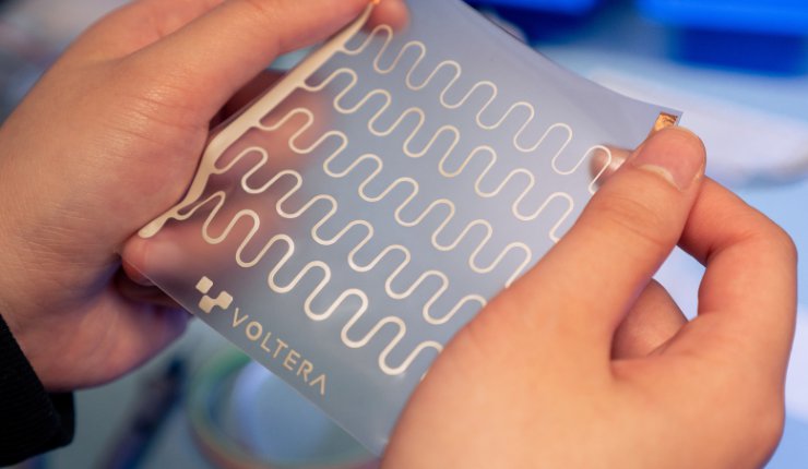
In 2022, Voltera, a leader in printed electronics technology, launched the NOVA, a new platform for printing flexible hybrid electronics. The NOVA uses direct write technology to print circuits on soft, stretchable and conformable surfaces. According to Voltera, the precision extrusion technology of the printer can help conduct research and develop ‘products of the future’.
The NOVA is capable of handling electrically conductive inks of high viscosity levels, which is how it creates flexible electronics. Copper and silver are the main materials that the team at Voltera works with, but an assortment of materials are capable of being handled by the NOVA system.
Jesus Zozaya, CEO and Co-Founder of Voltera, told TCT: “It’s a bench-top device that allows a designer, usually a researcher, to prototype an idea very quickly, probably in about an afternoon, and iterate very quickly as they test it out. We’ve got interest from different academic and research institutions from all over the world.”
Zozaya explained to TCT that in the field of additive electronics, there are typically two routes to go down. The first being the inkjet route, and the second being screen printing. Inkjet printing is typically limited to low viscosity materials that are very runny, such as water-based materials. Zozaya said that around 98% of printed electronics are created through screen printing.
Despite screen printing being very useful for high volume applications, the method has its challenges, according to Zozaya: “With screen printers you need a particular screen, which means that you need to get a new screen for every material, which if you are just getting started with a design, you’re not sure exactly what the final output will be like, and you can end up wasting a lot of resources. On top of that, screen printing in general can lead to a lot of wasted material, especially if you are working with inks that are very expensive. Some of our customers work with inks that have gold in them, so every tiny little droplet of the material is precious, quite literally, it’s a precious metal. So, what we find is that customers are attracted to our technology because it allows them to prototype with either materials that are very expensive or difficult to manufacture, but they’re still able to essentially work with the material with much less waste.”
The main benefits of the technology utilised in the Voltera NOVA is the weight savings and space savings that it provides. Zozaya says that in industries such as the aerospace and automotive industries, every gram that can be saved is important. The NOVA allows users to pattern different materials on what could be functional surfaces.
Zozaya added: “Imagine that you are printing a circuit on a big flat piece of PT that you will later form to give it the shape of whatever you need. The NOVA allows the electronics to be part of the design. Historically, you usually have the mechanical design and the electrical design, usually they are separated. So the mechanical engineer does the mechanics, the electrical engineer does the electronics and they’re usually working with a rigid board that’s made on FR4 and they meet in the middle with a couple of screws and some mounting hardware. Printed electronics allows those two domains to be married together at the start of the design, so it leads to a much more integrated design.”
Voltera works with a range of companies that are developing materials that can be used on the NOVA. Zozaya said materials are being developed by companies such as DuPont and Panasonic to name a few, as well as a number of smaller manufacturers. The CEO also said that the companies working with Voltera are pushing the limits of the different types of materials, as some can be conductive, some can be resistive, and some can be made for specific types of sensors.
In the initial announcement of the NOVA in late 2023, Voltera said “the future of electronics is flexible, which means the future of electronics is additive.” Zozaya told TCT that having the NOVA on your desk gives users a competitive advantage, as it has multiple functionalities and can fit on a benchtop in a lab or an office, which the company says saves money on the cost of tooling that would be associated with setting up screen printing.
Speaking about the future of the NOVA, Zozaya said: “The NOVA is kind of like a sandbox environment where different people can do different things with it. So, right now we’ve released two modules, one of them is our dispenser and one of them is a probe. The probe will allow height mapping of the surface, but we can develop additional modules that unlock different functionalities. One of them could be some type of a pick and place module that allows components to be placed accurately on the substrate. Another one could be a UV curing module, so if you’re dispensing some type of UV curable resin, then this module could come over and cure the resin that was dispensed. Another one could be some type of drill attachment or some type of laser drilling or laser curing as well, but there’s lots of opportunities for us to develop additional modules that would be more compatible in this machine, so it will get better over time as we develop more modules.”
In terms of the resolution of the prints that the Voltera creates, it is currently around 100 microns in terms of trace width, but Zozaya says the team is always working to improve that number, and it is a “never ending” goal for the company. As the resolution of prints using Voltera’s technology increases, more compact circuits and more complicated designs can be produced.
The primary material used for the NOVA is a silver-based conductive ink, which, according to Voltera, is an emerging field ‘actively being developed.’ Zozaya says there has been “huge” improvements in this area in the last two to three years. The new inks are more conductive and a lot more robust when it comes to soldering, according to the CEO, as well as being cheaper and having a longer shelf life. Zozaya emphasised to TCT that this technology will only improve over time.
Speaking to TCT about Voltera’s relationship with the companies that are producing the materials, Zozaya said: “I would say when we first started the company, we would send them an email and we were lucky if they replied. Now that relationship has changed a little bit and now we work pretty closely with a couple of suppliers to the point where they have manufactured custom formulations for us specifically. It’s very much like a partnership because we’re not in direct competition with them. We are making their jobs easier. We will recommend their inks to our customers and they’ll recommend our equipment to their customers.”
An example of a research project highlighted by Voltera to TCT was a customer comparing inkjet printing to extrusion printing, for the development of printed silver electrodes. According to Voltera, customers that are using the NOVA are primarily using the technology for wearable tech or biocompatible devices, but there have also been interesting applications for in-mould electronics and materials development.


